PcbComparer - PCB re-engineering software.
(c)2001-2022 Peacemaker.
PcbComparer
is the MS Windows software tool dedicated to investigate the radioelectronic circuits, the principle of operation of
various devices having the PCB - printed circuit board.
PcbComparer
is the graphic viewer of two pictures simultaneously, at the same time. Both
pictures should be the scanned sides of the one PCB. Instead of PCB viewing
with the naked eyes, PcbComparer enables to see the
both PCB sides in expanded scale simultaneously and to understand the principle
circuit of device.
PcbComparer
enables to enter the data of your device analysis to export the data of the
principle circuit and PCB-data of device (in the text format of CAD-program) to
design it further, if this information was entered by you manually.
16.08.2022
v.2.0.xx:
- author's contacts were updated;
- old shareware limitation were removed;
- “Export” menu error is fixed;
4.06.2005 v.1.3.xx:
- author's contacts were updated;
2.04.2002 v.1.3.xx:
- saving and editing of the traces was added;
- picture copying into clipboard was added: see the "Edit"-menu.
20.01.2002 v.1.2.xx:
- function of the trace filling was added.
8.01.2002 v.1.1.xx:
- scrolling step was decreased.
29.10.2001 v.1.1.xx:
- few errors was fixed;
- the sample was added.
Minimal system requirements:
1. MS Windows 95/98/NT/ME/2000/XP, Win 2010 is also compatible
2. Required library: %system_drive%\system\msvbvm50.dll (Visual Basic 5.0)
Program usage: Terminology
First see a terminology used in this description of the program (users who was
worked with electronic CAD-program (Protel, P-CAD, OrCAD, CircuitMaker ...) can pass
this terminology).
Good photos of a big resolution at vertical and horizontal axis are needed: 300
x 300 dpi – minimum (better 1200 x 1200 dpi plus).
Two pictures - images of top and bottom sides of PCB - let all petty details to
be visible.
Possibilities of PcbComparer:
1) Load two pictures of raster .bmp, .gif, .jpg format and view (scroll) of its
simultaneously.
2) Flip and rotate both loaded pictures to synchronization the location of
components and their pads.
3) Cursors and synchronization of cursors move, i.e. getting of correction
factor of cursor moving if pictures have different sizes, but both pictures
must be contrarotating.
4) Raster trace
filling (experimental function for 2005 year, funny in 2022).
5) Pads, their manipulations and properties.
6) Export the principal circuit (in the text format, .sch
file) end net-list (file .net) of Protel electronic
CAD-system (old version of Altium software).
1) PCB, board ... - printed circuit board.
2) CAD - computer-aided design, system (computer program) of automatic
designing of electronic devices (circuits, PCB, other documents).
3) Component, radio-element ... - electronic part of device with leads for
connection in circuit;
4) Component designator - the unique text name of the component in the electric
circuit
5) Sch lib reference, sch
component name ... - text name of component in the library of the images, which
will be drawn on the device principal circuit ;
6) Footprint, PCB lib reference ... - text name of component in the library of
the images, which will be drawn on the device PCB ;
7) Pad - the contact site for the lead of the component, they can have holes
through the PCB if leads are located vertically;
8) Pad designator - the pad name (usually it is the number of the lead of the
component);
9) Trace - flat metal (usually copper) path (the board was "printed",
you remember ?) for connection of pads ;
10) Net - the one point of electric contact of the leads (of the traces) of
components in the electric circuit
11) Net name - the name of the net, to which the pad is connected;
12) Via - through hole in board for connection of traces ;
13) Layer - individual level of PCB containing the traces; some layers connects
to other by means of vias;
Simple PCB have one layer only.
More composite PCB have two layers - "top" (side for placing of
components, but optionally) and "bottom" (usually for soldering leads
of component to pads), usually its use for not-complicated small computer
devices, i.e. this is majority of devices.
And very composite have three and more (computer motherboard...).
14) Net-list - the list of connections between pads on the PCB; there are
various CAD-formats of net-list containing the data of components, pads and
nets (but here used only one format).
Support:
©2001-2022 Peacemaker.
WWW-site: http://pmaker.ru
radioa@elec.ru
LICENSE AGREEMENT:
Usage of this software indicates your acceptance of this license agreement and
warranty.
UNDER NO CIRCUMSTANCES YOU MAY NOT REVERSE-ENGINEER, MODIFY OR ALTER IN ANY WAY
FILES OR PROGRAM ITSELF IN THIS
DISTRIBUTION PACKAGE.
You have the right to distribute the program freely.
Disclaimer of Warranty
THIS SOFTWARE AND THE ACCOMPANYING FILES ARE SOLD "AS IS"
AND WITHOUT WARRANTIES AS TO PERFORMANCE OR MERCHANTABILITY
OR ANY OTHER WARRANTIES WHETHER EXPRESSED OR IMPLIED.
ANY LIABILITY OF THE SELLER WILL BE LIMITED EXCLUSIVELY TO
PRODUCT REPLACEMENT OR REFUND OF PURCHASE PRICE.
Projects, save, load, close ...
Standard menu "File" - possibilities of load, save, save as ...,
close and create the new project.
At creation of the new project:
* first set new project file name;
* select file of first picture;
* select file of second picture.
Flip and rotate loaded pictures
Menu "Edit\Flip..." and "Edit\Rotate..." - this is a
possibility to flip or to rotate pictures for synchronization the location of
components and their pads: correspondence of contacts (pads) in the upper and
lower picture windows is required.
But for acceleration of current operation above the project it is better, if
these operations above pictures will be fulfilled by beforehand external
program (the graphics editor), before creation of the new project.
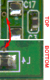
Menu "Edit\ Cursors move synchronization" -
this is an important function of the program: a clicked point must match the
correct point on the other PCB side.
But if pictures have different sizes - the cursor move synchronization is
needed, it is realized by means of a double set of cursors, see next 5 step:
1.Select menu "Edit\ Set the new cursors move scale"
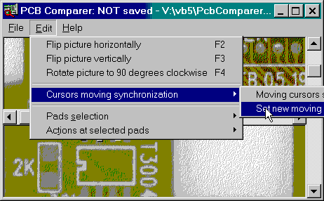
2.Set the first cursor (in top window) and next set the second cursor
corresponding to it, in the bottom window
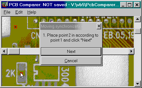
3.Click "Next" button

4.Set the second cursors pair for second synchronization point
5.Click "Done" button

But both pictures must be contrarotating.
Menu "Edit\ Cursors move scale 1:1" set the cursor move
synchronously, along equal coordinates of both pictures.
Pads: manipulations and properties.
1) At the mouse double click over the any picture (for example - above the pad
of the component) the small button will be placed on the picture (and on second
picture too will be placed the button correspondingly of first) - this is a
"pad".
2) It is possible to move (everyone individually) pads by means of the mouse
with the pressed and holding left button and Ctrl key.
3) Pads have properties:
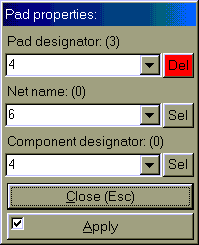
Between "(" and ")" - total quantity of :
* placed pads;
* entered nets names;
* entered components names.
"Del" button deletes the selected pad.
"Sel" buttons selects all pads with the
selected net name or all pads which belong to the selected component.
"Apply" button saves made changes to the properties of the selected
pad.
If several pads were selected - then the first changed property are to be saved
only to all selected components.
If the pad with unique properties is present already - then the
"Apply" button is disabled.
Set check box on the "Apply" button enables to leave in fields the
previous values of properties if properties of the following selected pad (-s)
- are not determined yet (are empty). This option is convenient for add of
group of consistently numbered pads (for example, at microchips).
Export the PCB data: the principal circuit and the PCB
net-list.
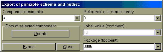
For each of components from the dropdown list you should set:
" the reference of sch library (for the principal circuit export);
" the part type
(label-value, comment), for example: manufacturer chip type
("LM193"), or the value of the electrical characteristic of the
component (in the some unit of measure, "10kOhm", "33nF"),
or simply the comment - "CENTRONICS CONNECTOR";
" the footprint (the
reference of PCB library, the package type of the component, "0805",
"SOD-80"...).
The export from the current version of the program is made into the text format
of CAD-system Protel.
The principal circuit is saved to the ".sch"-file
and the net-list is saved to the text ".net"
file.
The libraries of the current program version were exported from the CAD Protel 99SE version:
* Sch library -
"C:\Program Files\Design Explorer 99 SE\Library\Sch\Miscellaneous
Devices.ddb"
* PCB library - "C:\Program Files\Design
Explorer 99 SE\Library\Pcb\Generic Footprints\PCB
Footprints.lib",
where the "C:\Program Files\Design Explorer 99 SE\" is the folder,
where Protel 99SE was installed.
But it is necessary to be sure these 2 libraries which are used (see above), are connected to the project where you are going to
import the exported files.
Into the .sch-file is exported (in the current
program version) the components only, i.e. the defective principal circuit
which is destined for the PCB creation.
After export you can:
* to load the exported .sch
file into Protel 99SE version (create the new
project);
* to create the PCB by means "Design\Update
PCB" menu;
* to load into this new project .net-file (for
example, by means the drag-n-drop operation with net-file);
* to load into the created PCB the exported
.net file ("Design\Load nets" menu).
... and to work with the created project farther.
Good luck !
Trace filling (old function can be ignored).
This is a function of the region filling: click the point on the picture (over
trace, for example) and program automatically begins to fill the region which
contains clicked point: left mouse click at PRESSED ALT.
The region - is the color region. I.e. if the color of the
pixel belong to the defined range of the colors (ą percent of the number
of the initial pixel color) - this pixel should be re-painted to the filling
color.
The filling color defines the "Edit\ Tracing\Fill color" menu.
The range of the colors defines the "Edit\ Tracing\Color bound" menu.
This function can be useful for a mark of the long and tangled traces.